
High-Density PCB Board-to-Board: Stacking Pin and Female Headers Cleanly
Say which “dense” you mean
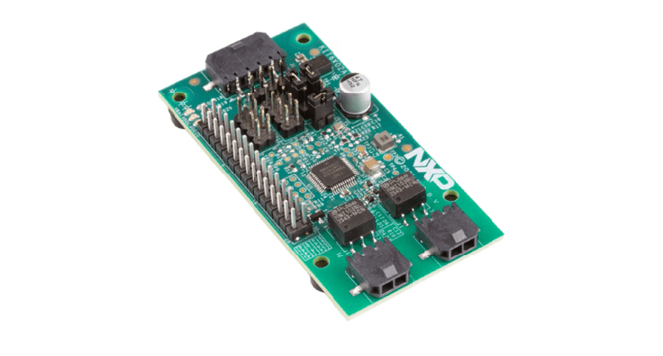
Phone board-to-board is often 0.4–0.5mm shielded floating parts for MIPI or PCIe. Industrial “dense” usually means the chassis got shorter and a 2.54mm 2×40P no longer fits, so control, comms and sense boards stack. Pin + female still works at 2.00 / 1.27 / 1.00mm with insulator height locking the gap. Public VFD, DAQ and gateway schemes look like this — not like a handset motherboard.
Three geometries
StackTypical partsTolerance that bitesParallel mezzaninePins on one board, socket on the otherHeight + pin length = gap; two connectors must share one hole gridRight-angle side entryRight-angle pin into a socketLid, wall and finger accessSOM into carrierA pin field on a moduleAsymmetric pegs so it cannot mate 180° out
Three failure modes
- Two connectors at once: a 2×20P plus a 2×10P power header 0.2mm off will float one side and bottom the other. One drill drawing, one supplier set.
- No side section: catalog pin length is not exposed length. Overlap the female contact 1.5–2.5mm. Tall caps hit the lid first.
- Open pins as a backplane: PWM, UART, GPIO, I2C yes; MIPI and SerDes need impedance-controlled BTB. Short stacks cut loop area; they are not transmission lines.
Pitch on these boards
Many signals, little current: 1.27mm or 1.00mm dual-row SMT, watch coplanarity and PA6T/LCP. Mixed signal plus a few amps: 2.00mm with paralleled power on the outside. Service by hand or wave solder: keep 2.54mm. 0.80mm exists on some VFD boards and punishes placement and rework — qualify force and coplanarity, not only area.
Junjia can ship matched pin/female sets with custom length and height. Send target gap, connector coordinates and which pins are power; we will map PAS/PAR/PAM plus the socket instead of forcing two catalog leftovers.